AI Designsthe OptimalAI Chip
Eliminating human inefficiency from semiconductor design. 8 AI agents autonomously optimize every transistor — from architecture to silicon.
The Problem
Human Bottlenecks
Chip design is slow, expensive, and full of human inefficiency
Human Bottleneck
Traditional chip design takes 2-3 years with hundreds of engineers. Manual iteration, siloed teams, sequential handoffs — human inefficiency at every step.
Prohibitive Cost
ARM licensing + massive teams + long cycles = $50M+ to tape out. Only giants can afford to play.
Closed & Rigid
Proprietary architectures, vendor lock-in, no cross-domain optimization. Each expert sees only their silo.
Our Solution
Let AI Do What AI Does Best.
AI Designs the Chip
8 AI agents replace siloed human teams. They debate, optimize, and iterate 24/7 — eliminating every bottleneck in the design process.
RISC-V — Zero Lock-in
No ARM licensing fees. Full architectural freedom. AI agents have complete control to customize every instruction for optimal performance.
AI-Optimized Silicon
Custom NPU with Systolic Array. Every transistor placement, power path, and timing closure optimized by AI — not human intuition.
Chip Architecture
RISC-V SoC with Custom NPU
A complete Edge AI SoC designed for automotive inference workloads.
RISC-V CPU
RV64GC core @ 1 GHz — fetches instructions and orchestrates data flow across the SoC.
NPU
Custom Neural Processing Unit with Systolic Array — handles INT8/FP16 matrix multiply for inference workloads.
AXI4 Interconnect
High-bandwidth on-chip bus fabric — connects all masters and slaves with low-latency arbitration.
SRAM
512 KB on-chip SRAM — provides single-cycle access for weights and activation buffers.
I/O & Periph
UART, SPI, I2C, GPIO — standard peripheral interfaces for sensor and actuator connectivity.
DMA
Direct Memory Access controller — moves data between SRAM and peripherals without CPU intervention.
Product Specifications
| Spec | Edge AI v1 | Edge AI v2 |
|---|---|---|
| Process | TSMC 28nm | TSMC 7nm |
| Array Size | 16 × 16 | 32 × 32 |
| Performance | ~1 TOPS | ~8 TOPS |
| Power | ~0.5W | ~2W |
| Data Types | INT8, FP16 | INT4/8, FP16/BF16 |
| Die Size | ~25 mm² | ~15 mm² |
| Target Price | $15–50 | $100–300 |
| Timeline | 2028 | 2030 |
4,480
lines
SystemVerilog Generated
10
modules
IP Blocks
8/8
pass
Tests Passing
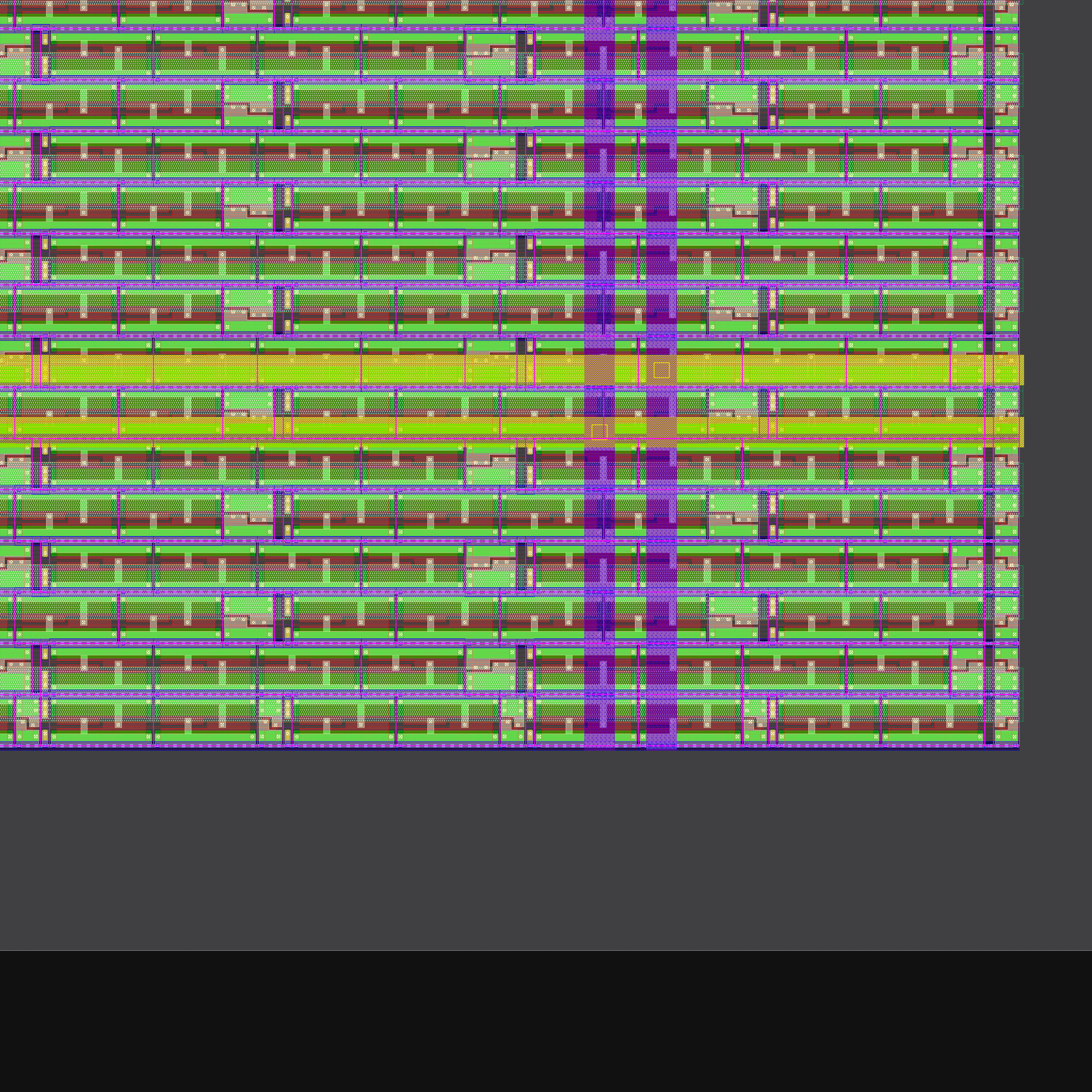
From RTL to Layout
Real Silicon — GDSII Generated
OpenLane flow with SKY130 PDK — 42 steps, DRC/LVS clean. 209 standard cells, 3mm x 3mm die, 50MHz.
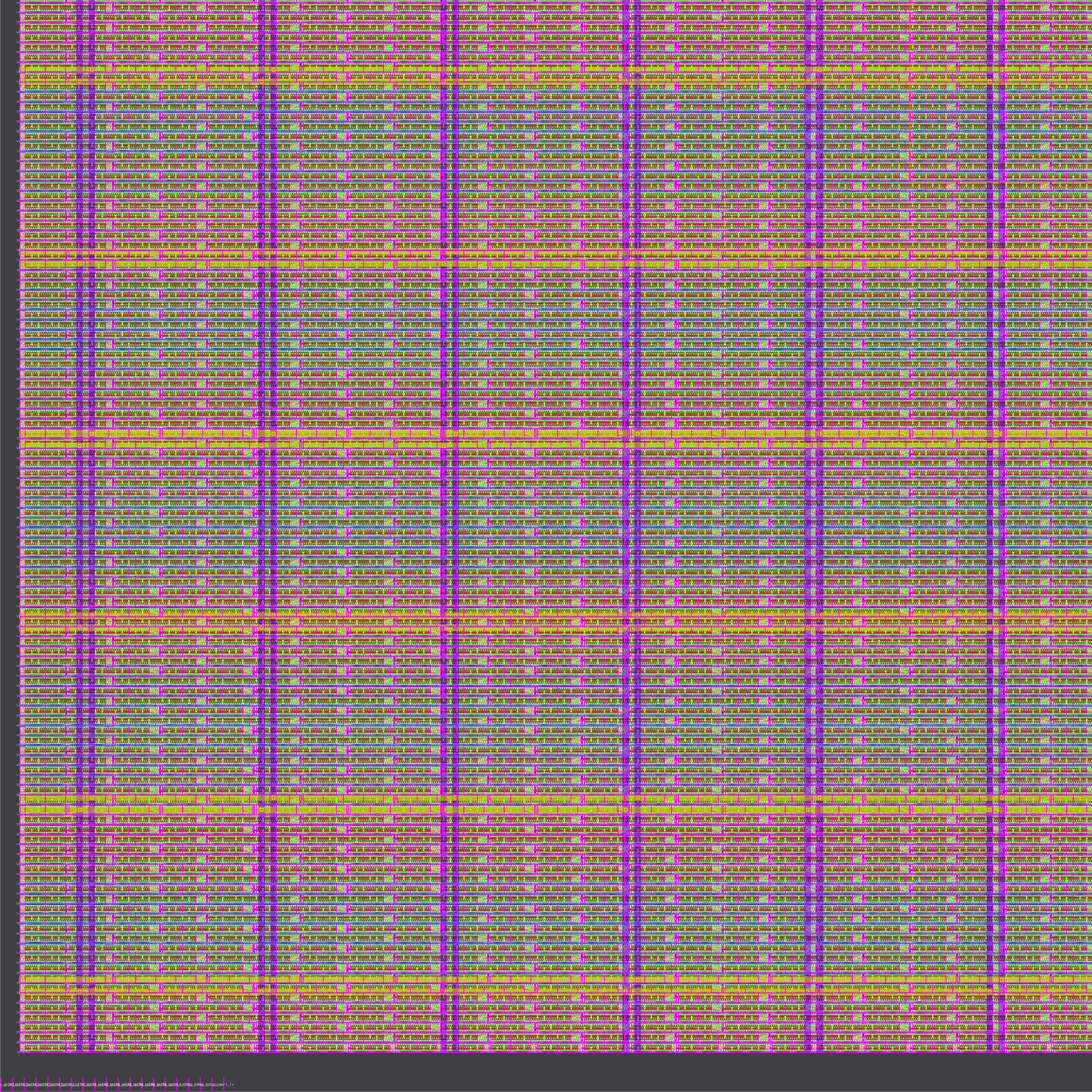
Full die with power distribution network
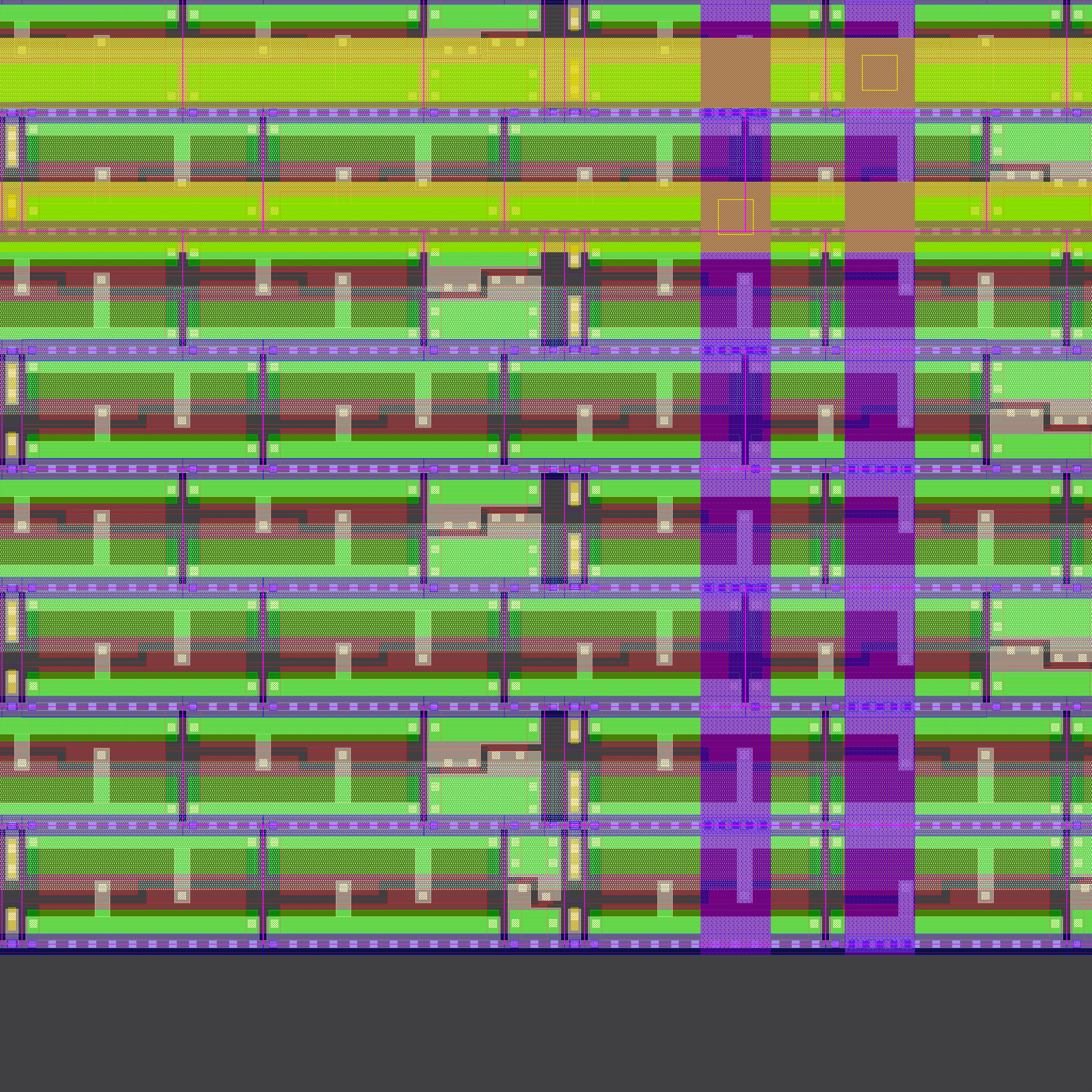
Placed & routed cell array with routing channels
Deep zoom into individual logic gates

Metal layers, vias, and diffusion patterns
Multi-Agent Design Council
AI Design Platform
No human handoffs. No siloed teams. No waiting. 8 AI agents autonomously debate, optimize, and iterate — producing silicon that no single human team could design.
Autonomous multi-agent deliberation
Architect
SoC structure & tradeoff analysis
RTL
Chisel/SystemVerilog code generation
Verify
Testbench & coverage analysis
Physical
Floorplan & timing closure
Power
Power analysis & DVFS optimization
Safety
ISO 26262 & FMEA analysis
Software
SDK, drivers & compiler optimization
Cost
Die area & yield analysis
The GitHub for Semiconductor Design
Open Design Protocol (ODP)
MCP-based open collaboration standard. External partners contribute specialized AI bots while IP security is maintained through sandboxed execution and digital NDAs.
Foundry Bots
TSMC, Samsung
EDA Bots
Synopsys, Cadence
IP Vendor Bots
SiFive, Andes
Customer Bots
Denso, Toyota
Standard Bots
ISO, JEDEC
IP Security Framework
Masked Context
Sensitive IP is tokenized and abstracted before sharing with external agents
Digital NDA
Cryptographic agreements enforced at the protocol level for every interaction
Sandboxed Execution
External bots run in isolated environments with no direct access to design data
Audit Trail
Every agent action is logged, timestamped, and traceable for compliance review
Powered by Claude API (Anthropic), LangGraph orchestration
Business Model
Dual Engine: Chip + Platform
Hardware revenue powered by high-margin SaaS — creating a valuation premium that pure semiconductor companies can't achieve.
Chip Sales
Automotive Edge AI inference chips (28nm → 7nm)
Margin 55-65%Platform SaaS
AI Design Council subscription + ODP platform access
Margin 85%+Bot Marketplace
Transaction fees from external specialist bot ecosystem
Margin 90%+IP Licensing & NRE
NPU IP licensing + custom chip design services
Margin 70%+Data Insights
Design trend analytics, benchmarking reports
Margin 90%+5-Year Revenue Projection
Revenue in $M — segmented by Chip, Platform, and IP/NRE
Total Addressable Market
Automotive Edge AI Chip
Semiconductor EDA / Design Automation
AI-based Design SaaS
Total Addressable Market
Valuation Comparison
$28.5M revenue x 5-10x multiple
$142M – $285M
$42M revenue x 15-30x SaaS multiple
$630M – $1.26B
Platform Subscription
Scalable pricing for every stage of growth
Starter
$1K/mo
- 4 internal bots
- Basic ODP access
Professional
$3K/mo
- 8 bots + 5 external
- Advanced analytics
Enterprise
$10K/mo
- Unlimited bots
- Custom setup & SLA
Product Roadmap
Building the Future, Phase by Phase
Chip
- TSMC 28nm HPC+
- 16x16 Systolic Array
- ~1 TOPS @ ~0.5W
- $15–$50 unit price
- ~25mm² die area
- INT8 / FP16
Platform
- AI Design Council MVP
- 8 internal bots
- Architect + RTL + Verify bot prototype
- LangGraph orchestration
- Claude API backend
- Real-time discussion UI
- Internal dog-fooding
Chip
- TSMC 7nm
- 32x32 Systolic Array
- ~8 TOPS @ ~2W
- $100–$300 unit price
- ~15mm² die area
- INT4/8, FP16/BF16
Platform
- ODP v1.0 launch
- 50+ partner bots
- External bot SDK
- Security framework
- 5–10 partners
- SaaS revenue starts
Chip
- TSMC 5nm / 3nm
- Next-gen NPU architecture
- 16+ TOPS @ <3W
- $50–$100+ unit price
- Multi-die chiplet
- Transformer acceleration
Platform
- Full GA
- Bot marketplace
- Subscription billing
- Data insights product
- 20%+ revenue from platform
Why Nagoya
Born in the Heart of Japan's Automotive Capital
Nagoya is home to Toyota, Denso, and the world's most concentrated automotive ecosystem. We're building where our customers live.
Automotive Hub
Direct access to Toyota, Denso, Aisin, and 400+ automotive suppliers. Same-day meetings with major customers.
Cultural Alignment
Deep understanding of Japanese business practices. Trust-based relationships with local OEMs and Tier 1 suppliers.
Cost Efficiency
30-40% lower operating costs vs Silicon Valley. World-class engineering talent at competitive rates.
Government Support
METI semiconductor subsidies, NEDO R&D grants, JIC investment program, and Aichi Prefecture startup support.
Talent Pipeline
Nagoya University and NITI produce top-tier engineers. Strong semiconductor research ecosystem.
Strategic Location
Central Japan — equidistant to Tokyo and Osaka. Gateway to Asia-Pacific automotive markets.
Target Customers
Technology Partners
Japan Funding Ecosystem
METI Semiconductor Subsidy
National semiconductor strategy with multi-billion dollar subsidies for domestic chip development and manufacturing.
NEDO R&D Grants
Government-backed research grants for advanced technology development including AI and semiconductor innovation.
JIC/INCJ
Japan Investment Corporation providing strategic investment in next-generation semiconductor startups.
Aichi Prefecture Startup
Regional support programs offering subsidies, office space, and networking for technology startups in Nagoya.
Toyota/Denso CVC
Corporate venture capital from automotive leaders actively investing in automotive semiconductor innovation.
Traction
Development Progress
Real engineering milestones. Not just a pitch deck.
Chip Development
7/11AI Platform
3/7Business
1/3Contact
Interested in partnering?
Whether you're an investor, automotive OEM, or technology partner — we'd love to hear from you.
contact@nagoyasemi.com